
Semiconductor PEEK Components
Semiconductor PEEK Parts
Custom CNC machined PEEK components for semiconductor equipment, high-temperature fixtures, insulating parts, and precision engineering plastic applications.
Material Selection
Why PEEK Is Used in Semiconductor Equipment
PEEK is often reviewed for semiconductor equipment because it combines useful temperature resistance, dimensional stability, chemical resistance, electrical insulation, low moisture absorption, and practical machinability for precision components. These properties make PEEK suitable for many structural, insulating, fixture, and handling parts where metal may not be preferred.
Final material selection should still depend on the grade, part geometry, tolerance requirements, surface finish, chemical exposure, and operating conditions. For higher load or wear requirements, engineers may also compare PEEK with PAI / Torlon machining options.
Typical Components
Typical Semiconductor PEEK Components
Wafer Handling Fixtures
Drawing-based PEEK fixtures for controlled handling, positioning, and repeated assembly use.
Insulating Blocks
Electrical insulating PEEK components for equipment structures, mounts, and support blocks.
PEEK Spacers
Precision spacers, sleeves, standoffs, and distance-control parts machined to drawing.
Sensor Mounts
Stable plastic mounts for sensors, probes, and inspection-related equipment assemblies.
Vacuum-Compatible Plastic Parts
PEEK parts reviewed for vacuum-related use where geometry, cleanliness, and material grade matter.
Chemical-Resistant Components
Custom PEEK parts for chemical exposure areas, depending on reagent and process conditions.
High-Temperature Positioning Parts
Positioning plates, guides, and supports used near elevated-temperature process zones.
Custom Drawing-Based PEEK Parts
Prototype and small-batch PEEK components produced from CAD, drawings, or sample requirements.
Machining Review
CNC Machining Considerations for PEEK
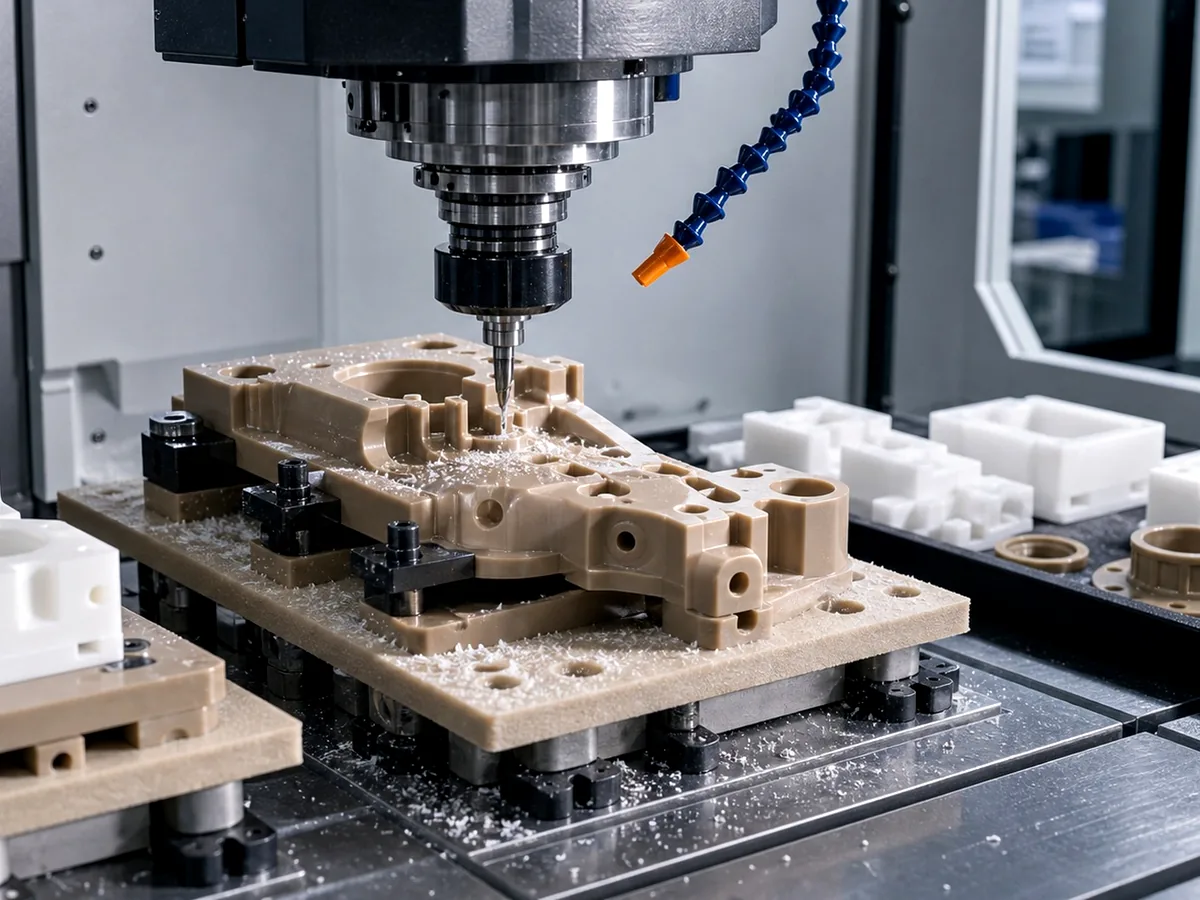
PEEK CNC machining requires attention to tool sharpness, chip evacuation, burr control, clamping force, and heat management. Thin walls, sharp internal corners, deep pockets, and tight hole-position requirements should be reviewed before quotation.
- Use appropriate tooling and cutting strategy to reduce burrs and heat buildup.
- Review warpage risk for thin sections, asymmetric pockets, and high material removal.
- Avoid unnecessary sharp corners where fillets can reduce stress concentration.
- Confirm tolerance strategy for prototypes, small batches, and repeated production lots.
Materials and Alternatives
Materials and Alternatives for Semiconductor Plastic Parts
PEEK is a strong starting point for many semiconductor plastic parts, but it is not the only material to review. Depending on wear, temperature, chemical exposure, dielectric requirements, and cost, alternatives such as PAI / Torlon, PEI, PTFE, and PPS may be more appropriate.
Inspection
Quality and Inspection
Micrylix reviews drawings before machining and checks critical features according to project requirements. Inspection focus may include dimensional checks, tolerance verification, surface finish review, hole and thread checks, and small-batch repeatability.
Drawing Review
Material, geometry, tolerances, surface finish, and inspection points are reviewed before quotation.
Tolerance Verification
Critical dimensions, hole positions, flatness, and mating features can be inspected against drawings.
Repeatability Support
Prototype and small-batch PEEK parts can be reviewed for process consistency and production risk.
RFQ
Need Custom PEEK Parts for Semiconductor Equipment?
Send your drawings, material requirements, quantity, tolerance requirements, and application conditions. Micrylix will review manufacturability and provide a quotation.